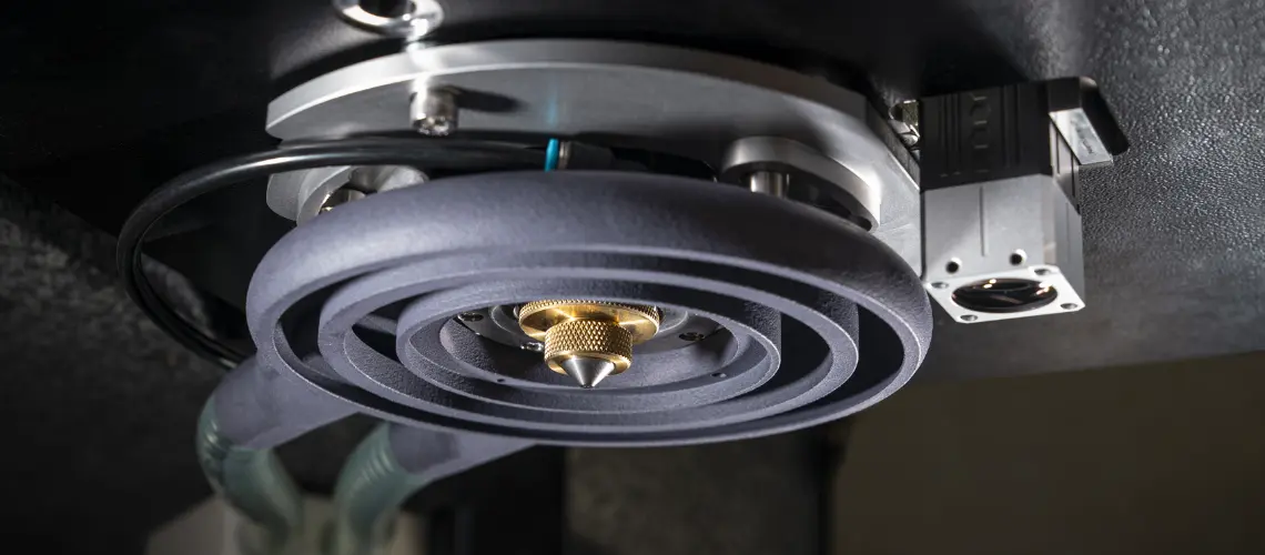
Probe card guide plates micro-drilling for semiconductors wafer testing industry
Probe card guide plates in semiconductors wafer test industry faces the challenge of ensuring very high accuracy and stability. With the miniaturization and increasing complexity of integrated circuits, the plates must smoothly guide each probe to its exact test point on the wafer. Any weakness can compromise the test reliability or even harm the device under test (DUT). As wafers evolve with a denser quantity of microchips, the development of advanced probe cards must constantly anticipate this progress. The probe head containing the guide plates must be robust, enduring countless test cycles while retaining its precision.
Probe cards guide plates micro-drilling application overview
We process any kind of probe card guide plates on a wide range of ceramic materials (Si3N4, Photoveel, etc.). The hole shape is programmable; round, square, rectangle, oblong holes, the possibilities are endless. A very low taper or “zero taper” is required for very fine pitch to avoid hole break-through. Utilizing a process characterized by a high repetition rate and unmatched Laser beam quality, it promises exceptional repeatability in hole quality. This meticulous approach not only delivers unequaled productivity but also ensures a higher yield rate. Critically, the entire process is free from thermal effects (NAZ), safeguarding the integrity of the material at every step.
Probe cards guide plates micro-drilling application overview


Achieved results
A micro-drilling project for probe cards guide plates needs a high degree of commitment on tight specifications. On this basis, our results meet (or exceed) market requirements:
- Drilling diameters down to 20 μm
- Positioning accuracy ± 2 μm
- Wall thickness (between two holes) < 10 μm
- Corner radius (for square/rectangle holes) ≤ 3 μm
- Hole size accuracy < ± 2 μm
- Aspect ratio 1:10 (or higher depending on material and hole shape)
You currently have a probe cards guide plates drilling project and you would like to know what we could achieve together?
Give us some more details!
The FEMTOsecond LASER technology is a perfect match for all industries requiring the highest precision without compromising quality and productivity.
Miniaturized components are used in all kind of devices. Several applications – e.g. in the electronics or MedTech world – are not imaginable without very small and tiny parts. Thus, this requires new ways to produce and manufacture these parts. With FEMTO LASER μ-machining there are various processes possible like drilling, cutting and turning. It's compatible with almost all materials that are otherwise very difficult to machine with conventional tools.
With each FEMTOsecond LASER pulse that hits the work-piece, a small amount of material immediately vaporizes. The material removal occurs in a controlled manner leading to no damage, burrs or any negative influences to the material integrity.
Your benefits:
- FEMTOsecond Laser source < 300 fs
- Highest level of accuracy and productivity
- Stable and repeatable quality
- Cold ablation keeping material integrity (no HAZ)
- Proven performance in 24/7 industrial environment
FEMTOsecond LASER machines provide advanced µ-machining solutions for high-tech production. It ensures impeccable surface smoothness and precise machining without thermal residue.
Other applications that might be interesting for you

Turning of contacts pins for IC substrates testing industry
Turning of contact pins (wires, bars and tubes) for semiconductors testing industry
Drilling and routing of composites and non-ferrous materials for printed circuit boards (PCB) industry
Let’s discuss your micro-machining operations
If you are looking for a high-tech production system as well as a partner to process state-of-the-art micro-machining, you are in the right place.